Why 48V Architecture? (Key Benefits)
The 48V architecture’s core principle is to’ increase voltage while maintaining power output to reduce current’, delivering a series of key advantages:
1.High efficiency, low loss:
According to the DC power formula P = V × I, when the power remains constant, the voltage increases fourfold (from 12V to 48V), while the current decreases to one-fourth of its original value.
According to Joule’s law, the heat loss in a wire (P_loss = I² × R) is proportional to the square of the current. When the current is reduced to one-fourth, the line loss decreases to one-sixteenth of the original, significantly improving energy efficiency.
Lightweight and low-cost:
Smaller currents mean thinner wires (with smaller cross-sectional areas) can be used.
This directly reduces the weight of the system’s cables and material costs, which is crucial for weight-sensitive fields such as automotive and robotics.
3.High power density:
For robotic devices, smaller motors and thinner cables enable more compact and lightweight joint designs, enhancing both flexibility and integration.
Security and Inheritance:
48V serves as the maximum safe voltage in typical applications, eliminating the need for stringent electrical safety measures and thus reducing system complexity and costs.
It is a natural evolution of existing low-voltage systems (12V/24V), maintaining technical continuity (with lead-acid batteries rated in multiples of 6V).
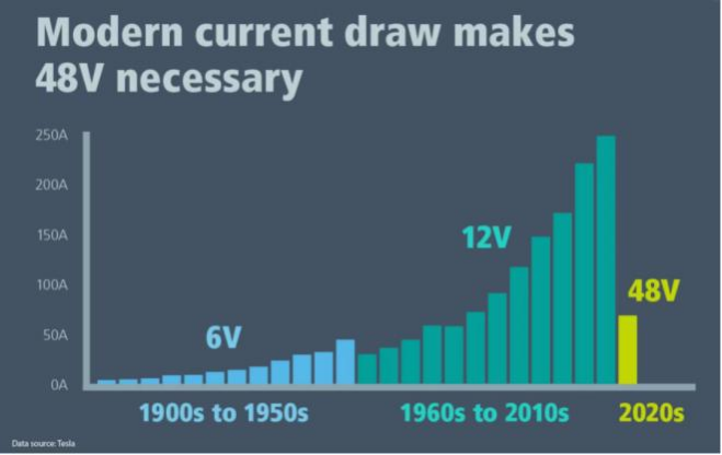
Review of the Development History of 48V Architecture
Development line: from meeting basic needs to pursuing extreme efficiency, application field from fixed facilities to mobile platform.
Early standards (early 20th century): 48V DC became the standard voltage for fixed telephone central offices, laying the foundation for modern telecommunication networks.
The evolution of the automotive industry:
6V era: Three 2V lead-acid batteries connected in series, which was the early standard.
12V Era: With the proliferation of in-vehicle electrical systems and rising power demands, the configuration evolved to six batteries connected in series (6V×2).
24V Era: Commercial vehicles, due to their high power demands, adopt a 12-cell series battery configuration (12V×2) to reduce current and improve efficiency.
Data Center Revolution (circa 2016): Spearheaded by Google and the Open Compute Project (OCP), this initiative addressed the massive power consumption of servers by implementing 48V power distribution, which significantly reduced energy waste and operational costs.
Automotive Breakthrough (2023-2024): Tesla’s Cybertruck became the first production vehicle to fully adopt a 48V powertrain, replacing the decades-long 12V system and demonstrating its immense potential in mobile platforms.
Robotics adoption (since 2020): Industrial, logistics, and service robots have adopted the 48V architecture to achieve higher efficiency, lighter weight, and more compact designs.
The inaugural year of humanoid robotics (2024): Leading manufacturers including Tesla’s Optimus and XPeng’s IRON have all adopted the 48V battery architecture, establishing it as the new benchmark for advanced mobile robotics platforms.
The 48V architecture serves as the foundational cornerstone for robots to achieve “compact size, extended battery life, and intelligent interaction”.
Why GaN is the Preferred Motor Drive Solution? (Key Advantages)
GaN (gallium nitride) chips, with their core advantages of low loss and high power density, have overcome the limitations of traditional silicon-based devices, emerging as the key development direction for medium and low-voltage motor drives. The core advantages of GaN chips include:
Low switching loss:
Zero reverse recovery characteristic, no tail current, low switching loss of capacitor, optimized voltage-current overlap loss, significantly reduce the total loss of the system.
High-frequency adaptability:
It supports higher PWM frequency (far exceeding the 6-16kHz range of silicon-based devices). The frequency increase results in minimal power loss increment, effectively reducing motor current ripple and torque ripple while enhancing control precision.
High power density:
It enables smaller passive components (inductors and capacitors) to achieve higher output current under the same conditions, supporting greater loads.
Tough environment and fast response:
It features low temperature rise, superior thermal resistance, rapid dynamic response, and adaptability to complex operating conditions.
Comparison of Core Parameters of GaN and Si-based (IGBT/MOSFET) Motor Drivers
contrast ratio
GaN-based motor drive
Si-based motor drive (IGBT/MOSFET)
I. Basic Characteristics of the Materials
energy gap
3.4eV (wide bandgap, high temperature and high pressure resistant)
1.12eV (narrow band gap, low tolerance limit)
heat conductivity
Approximately three times that of silicon (high thermal conductivity)
Reference value (approximately 150W/(m·K), with weak conductivity)
electron saturation velocity
2.8×10⁷ cm/s (high-frequency switching supported)
Approximately 1×10^7 cm/s (high-frequency performance limited)
II. Switch Performance
maximum switching frequency
Supports MHz level (typically 100kHz+; some scenarios reach MHz)
Rated at 20kHz, but typically operates between 6-16kHz (high-frequency operation causes significant power loss)
reverse recovery charge
Zero (no reverse recovery loss, supports high di/dt/dv/dt switching)
IGBT requires parallel diodes, which still incur reverse recovery loss; MOSFET’s body diode has a high Qrr.
dead time
Minimum 14ns (reduces torque harmonics and vibration)
100-500ns (may cause current discontinuity, leading to sixth-order torque harmonic)
III. Loss Characteristics
Switching loss reduction (compared to silicon)
Discrete regimen reduced 39%(11.6w vs 19w), combined regimen reduced 24.5%(12.3w vs 16.3w)
Baseline value (high frequency causes high loss ratio, limiting efficiency)
frequency enhancement loss increment
The power increase is only 0.7W when the frequency is increased from 20kHz to 40kHz, with the loss increment reduced by 83%.
The power output increases by 4.1W when the output power is increased from 20kWz to 40kWz (with loss significantly increasing as frequency rises).
On-resistance (RDS(on))
Based on two-dimensional electron gas (2DEG), it is far lower than silicon devices under the same specifications.
The on-resistance (RDS) of MOSFET increases with current and temperature, while IGBT maintains a constant saturation voltage but exhibits tail current loss.
IV. Thermal Properties
device thermal resistance (Rth (i-s))
As low as 0.5K/W (flip-chip/CCP, short thermal path)
1.5-2K/W (traditional package with low heat dissipation efficiency)
Differences in junction temperature with the same power consumption
Low body temperature (20-40℃) (rapid heat conduction, minimal heat accumulation)
The temperature is too high and may trigger overheating protection
Demand for heat sinks
No heat sink required for devices below 200W; the 1kW sealed package solution eliminates the need for a heat sink when current is below 18A.
Medium and low-power systems still require heat sinks, while high-power large-scale cold air/liquid cooling modules
V. System Design Features
Volume of passive components
Replacing 330μF electrolytic capacitor with 22μF ceramic capacitor reduces inductor size (lowering capacitive-inductive requirements at high frequencies).
Rely on large volume electrolytic capacitors and inductors (requiring current ripple simulation at low frequency)
Power density (output current)
The discrete solution delivers 3.5A higher effective current value ratio (Si) while supporting greater load capacity at identical temperature rise.
Reference value (current boost limited by power loss and heat dissipation)
electromagnetic interference
High integration (e.g., half-bridge sealed), allowing internal motor embedding to reduce cable length and minimize EMI.
Discrete layout, long cable length, strong EMI radiation at high frequency
VI. RELIABILITY
temperature tolerance
The temperature tolerance is far superior to that of Si-based devices (stabilizing operation under high load)
Low temperature tolerance, life shortened at high temperature
device lifetime (Arrhenius model)
Life doubles for every 10℃ drop in junction temperature (lower junction temperature prolongs lifespan)
High body temperature and relatively short lifespan
Mean Time Between Failures (MTBF)
Higher (low loss + low thermal stress, reducing failure risk)
Lower (higher thermal stress and failure probability due to wear)
Typical manufacturers and solutions of GaN
TI DRV7308
Integrated GaN FET pre-driver with three-phase modulation and field-oriented control capability.
12mm× 12mm QFN package, with over 99% efficiency in 250W motor drive applications, eliminating the need for a heat sink.
Innosense Low-Voltage Solution (48V-60V Input, Compatible with 1kW Class Motors)
Discrete scheme (INNDMD48V25A1): 6 INN100EA035A+3 INS2003FQ, the total loss is 11.6W (Si scheme 19W) at 40kHz/20A, and the temperature rise is only 10℃ when the frequency is increased to 40kHz.
Encapsulation scheme (INNDMD48V22A1): 3 ISG3204LA half bridge GaN encapsulation, total loss 12.3W (Si scheme 16.3W) at 40kHz/20A, no radiator is needed below 18A.
Companies including Texas Instruments (TI), Infineon, Innosense, EPC, and Nanoware are actively developing applications of gallium nitride (GaN) in humanoid robots, particularly for motor drive systems.